We architect microcontroller subsystems around a RISC-V core, focusing on a clear bus fabric, a robust clock and reset strategy, and resource-aware RTL. Each design ships with timing reports, register maps, and bring-up notes, so it stays portable across FPGA families and open PDKs.
The shape of the design
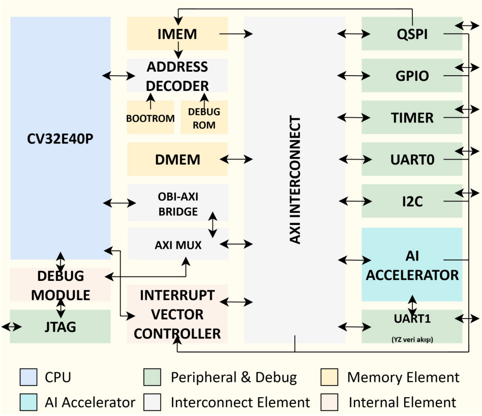
A CV32E40P core issues memory-mapped reads and writes over an in-house AXI4-Lite interconnect. A central address decoder picks the target peripheral from the transaction address. Because every peripheral presents the same AXI4-Lite slave interface, adding one means adding a decode range and a slave — the core itself never changes.
The full module map lives on the architecture page.
Bring-up, one version at a time
Rather than integrating everything and debugging a black box, the design advanced through a sequence of numbered demo milestones. Each one adds peripherals or fixes on top of a version already known to run on hardware, so when something breaks the search space is one increment wide. The timeline on the home page tracks where that sequence currently stands.
What ships with each block
- Synthesizable SystemVerilog RTL
- Register map and documentation
- Timing and resource reports
- A directed testbench with assertions
Next
With the final hardened run behind us, the focus has moved to documentation and integration examples. This post will expand with concrete numbers — utilisation, achieved clock, and per-peripheral resource cost.