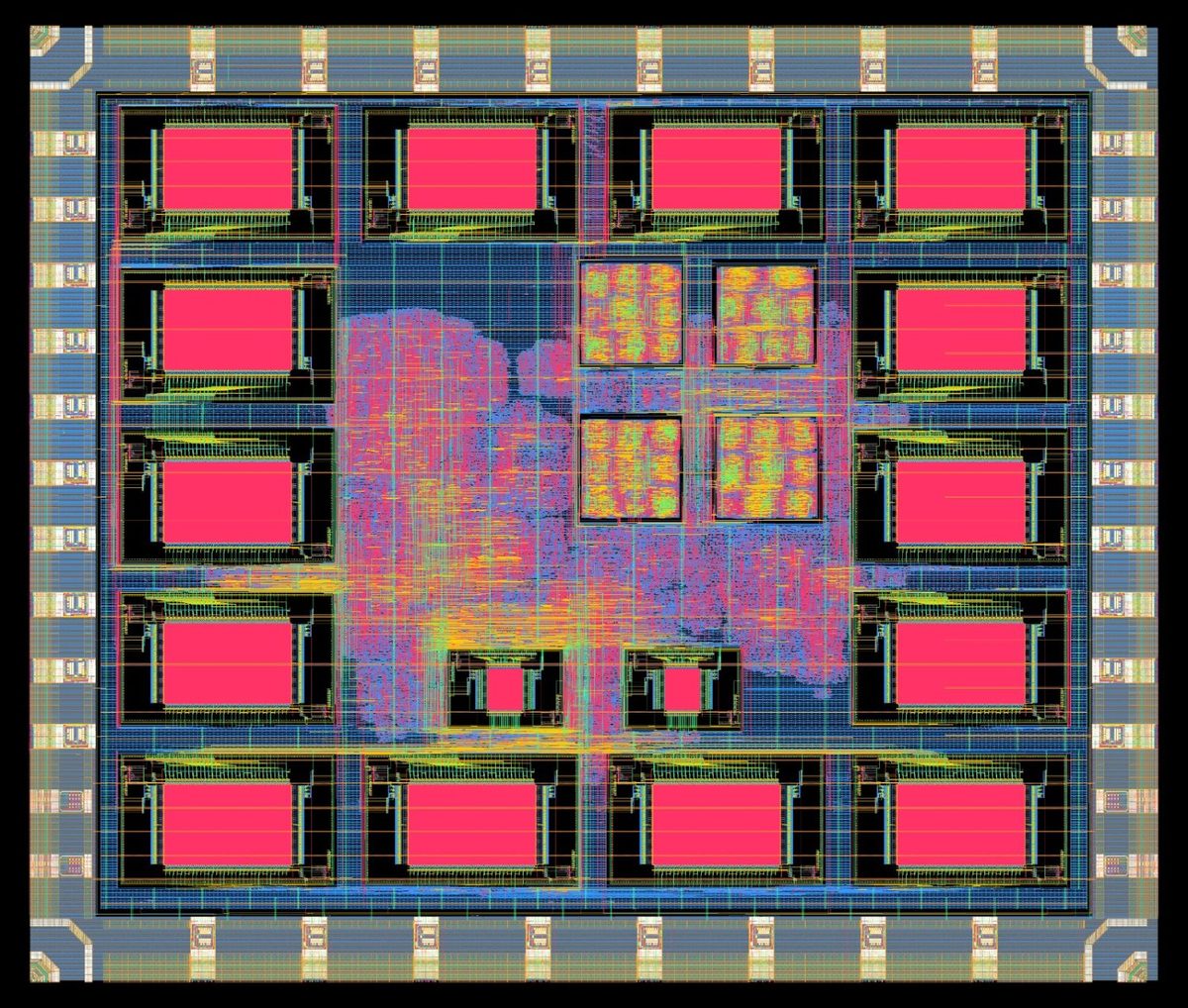
SKY130A is the open process design kit behind both hardened runs: the
standalone MCU on the demo_v04 design, and the full top-level
SoC — AI accelerator included — after demo_v10.
Floorplanning, macro placement, power ring and routing are all part of those
runs.
It is open in the sense that matters for a student team: no licence, no NDA, and a flow that can be re-run from a clean checkout.
Results
The hardened design closes at 71.4 MHz on a 130 nm process, drawing 110 mW in the core, across 60,249 cells and 8,065 registers. It is signoff ready.
Worth putting next to the FPGA numbers: the same RTL runs at 36 MHz on the Gowin part, so an open 130 nm flow reaches nearly double the clock of the low-cost FPGA it shares a design with, at well under half the power. The full three-way comparison is in High Performance, Cheap ASIC.